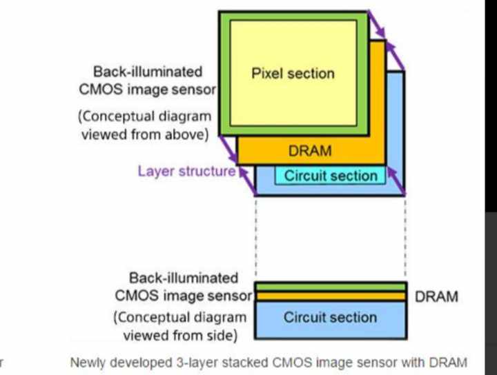
While conventional stacked CMOS image sensors consist of photodiodes and pixel transistors that reside on the same substrate, the new stacking technology allows for more optimization in both photodiode and pixel transistor layers.
This new technology allows for a wider dynamic range, double the saturation signal level, and reduce noise.
The stacked image sensor design also allows for the pixel transistors to be larger, which Sony says will improve battery life and the resolution of the photos.
Earlier, the stacked CMOS image sensor was only capable of capturing a few megapixels. With this new method, a pixel has multiple layers of transistors, which allows for a higher quality image.
This new technology will be unveiled by the company in the event of IEEE (International Electron Device Meeting) that was held on Dec 11, 2021.
As a result, Sony’s stacked CMOS image sensor now contains two-layer transistors that enable it to capture high-quality, low-noise images even in low-light settings.
Also Read- IQOO Neo 5 SE Smartphone Specs Out- Launching on 20 Dec
Sony to make Stacked Image Sensor Technology more Advanced- Glimpse
The stacked CMOS image sensor also employs a back-illuminated pixel structure and a proprietary global shutter function.
The camera company says that the stacked CMOS image sensor has 12 effective megapixels, which is significantly higher than previous versions of the stacked CMOS format.
The new sensor design is based on an original Sony stacked event-based vision sensor. Unlike its predecessor, the new sensor features two layers of pixels, enabling high-speed, low-latency data output.
The technology would also allow cameras to detect a more complex scene. With such a high-speed and low-latency data output, a stacked image sensor will provide much higher-resolution images and reduced noise.
Besides developing new products that use the stacked CMOS image sensor, the company also plans to introduce a smartphone that utilizes the stacked CMOS image sensor in its smartphones and digital cameras.
Also Read- OnePlus achieved 10 million unit global sales target very early
Sony to make Stacked Image Sensor Technology more Advanced- Key Details
The two-layer CMOS sensor features a dual-transistor pixel structure that is referred to as a “double-pixel” camera. As the name suggests, the pixel size is a double-layer transistor.
In addition to stacked CMOS image sensors, Sony has recently developed a new architecture that has two layers of pixel transistors and photodiodes. This allows for better pixel performance, and doubles the saturation signal.
Ultimately, the sensor’s new architecture improves the dynamic range, which is the key to high-resolution images. If the new technology is successful, it will become the standard for CMOS-based cameras.
In addition to a new camera sensor, Sony will develop a hybrid CMOS image sensor, which will use a single CMOS image sensor and an AI-based processing system.
The stacked CMOS image sensor will be the world’s first to feature a two-layer pixel structure, which enables it to double its light-gathering capacity. The stacked CMOS pixel structure allows for more space for photodiodes and transistors.
Also Read- BGMI teased New Crossover with Sony’s Spiderman No Way Home
Sony to make Stacked Image Sensor Technology more Advanced- Wrap Up
The new technology enables the use of a 2-layer pixel structure. The two-layered CMOS image sensor provides twice the light gathering capability in comparison to a single-layer CMOS image sensor.
The stacked CMOS technology enables the production of smartphones with higher quality photos than a single-layered sensor. This is why smartphones and digital cameras use stacked CMOS sensors.
While conventional stacked CMOS image sensors have photodiodes and pixel transistors on the same substrate layer, Sony has separated the two layers using a proprietary stacking technology.
This new CMOS sensor has a higher saturation level and wider dynamic range. Moreover, it has a lower noise level. Its new design also improves efficiency by eliminating transfer gates. The resulting pixel is much smaller than the traditional CMOS sensor.
The new technology can improve image quality and low-power consumption. Its two-layer stacked structure makes it possible to save power and improve battery life. Moreover, the sensor is designed for smartphones. The technology will also improve the image-quality of mobile devices.
It is expected to be used in smartphones and other consumer electronics. But there are some limitations to its use in high-end cameras. However, the technology is promising.
Also Read- Apple to Start Making its own Chipset for 5G & Wi-Fi Compatibility

